Random Access Memory (RAM)
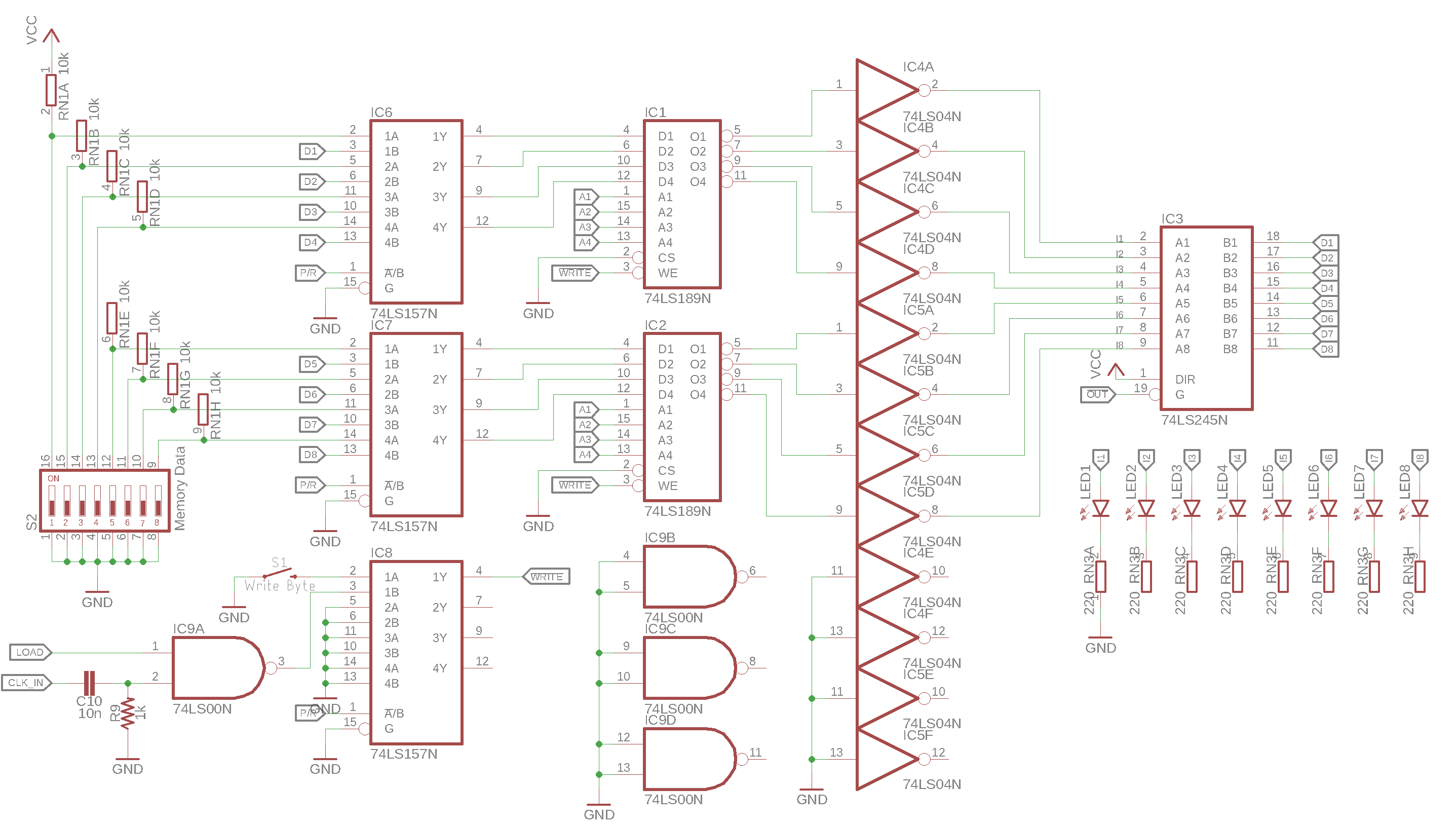
The RAM module allows to store up to 16 bytes of arbitrary data and access it by addressing the byte number in any order (random) rather that only one after the other (sequential).
The SAP-1 implements a von Neumann architecture which means there is only a single memory for instructions and data, thus both, the program and all data neccecary need to be stored in the 16 bytes of RAM.
Mode of Operation
The actual RAM storage is implemented using 2 seperate 74LS189 64 bit RAM with tristate output ICs (\(\mathrm{RAM\colon IC_1}\) and \(\mathrm{RAM\colon IC_2}\)) which are organized as \(16 x 4\) bit, thus each IC will be responsible for one nibble of the data byte.
For whatever reason, the 74LS189 chips have an inverted output, thus 2 additional SN74LS04 hex inverters (\(\mathrm{RAM\colon IC_4}\) and \(\mathrm{RAM\colon IC_5}\)) are used to flip the logic of the output again.
To be able to visualise the RAM contents at any address without needing to drive the databus, the same 74LS245 buffer that is used in the data registers is inserted between the RAM IC outputs and the databus lines.
The RAM Module needs to support 2 modes of operation which are selected by the \(P/R\) signal which is generated by the Memory Address Register module.
Program Mode
In program mode, bytes of data can be written to RAM by setting DIP switches representing the 8-bit value.
The program mode is selected by clearing the \(P/R\) signal which setups the 3 74LS157 quadruple 2-to-1 multiplexers (\(\mathrm{RAM\colon IC_{6-8}}\)) to select the A inputs and replicate their states on it’s outputs.
\(\mathrm{RAM\colon IC_{8}}\) is only used to select a single data-line which is connected to the \(\overline{WE}\) (write enable, active low) pins of the register ICs. Input 1A of this IC is connected to the tactile button Write Byte that pulls the line low when pressed, thus writing the current inputs to the selected RAM address. The button presses are not debounced, since multiple writes of the same value to the same address do not cause unwanted side-effects.
Run Mode
In run mode, the module read or write the databyte addressed by the Memory Address Register (MAR) to the databus (DB).
In run mode, the \(P/R\) signal is driven high, thus selecting the B inputs of the multiplexers. For \(\mathrm{RAM\colon IC_{6}}\) and \(\mathrm{RAM\colon IC_{7}}\), the B inputs are connected to the databus, thus pulling the \(\overline{\mathrm{WE}}\) line low in run mode will write the current byte on the DB into the selected RAM address.
The write line is set by NANDing the the \(\mathrm{LOAD}\) and \(\mathrm{CLK}\) signal thus the byte is written on a clock-edge and an active \(\mathrm{LOAD}\) signal.
To only write the byte on the rising edge of the clock signal, the signal is filtered by the RC high-pass built by \(\mathrm{RAM\colon C_{10}}\) and \(\mathrm{RAM\colon R_9}\). This is neccesary to avoid writing the state at the very end of the clock signal which could cause a race condition with whatever module is setting the DB state.
Schematic